
IRACE Version 2 Interfaces
Providing Detector Clocks:There are 16 clocks on each CLDC. Voltage levels are between plus and minus 10 volts, continuous current per channel is 20mA, peak current with 10% duty cycle and maximum duration of 100*s 80mA. Clock rise nad fall times are 50ns. |
 |
|
|
|
||
Providing Detector Clocks:There are 16 DC voltage on each CLDC. Voltage levels are between plus and minus 10 volts, continuous current per channel is 20mA, peak current with 10% duty cycle and maximum duration of 100ms 80mA. The output of CLDC board (BIAS and CLOCK) can be disabled either by software or by hardware. To disable the output by hardware the pin 36 of dsub p3 must be shorted to ground. By default the value of that pin is high (pull up resistor), that means the output can be enabled or disabled by software, otherwise the output is always disabled as long as that pin is shorted to ground. |
 |
|
|
|
||
Monitoring of output Clocks:MCh1: Output of the first channel monitor. Push the white button to change to the next channel. The selected channel number is shown by the green color led in binary format. MCh2: Output of the second channel monitor. Push the white button to change to the next channel. The selected channel number is shown by the yellow color led in binary format. |
 |
|
|
|
||
 |
|
|
Fiber optic cableUp to 2 Km fiber cable for the interface between frond-end electronics and back-end. |
 |
|
|
|
||
VME64 is a mechanical and electrical 'superset' of the original IEEE 1014-1987 standard. It offers new features such asLarger, 64-bit data path for 6U boards. |
 |
|
|
|
||
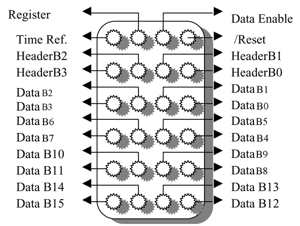
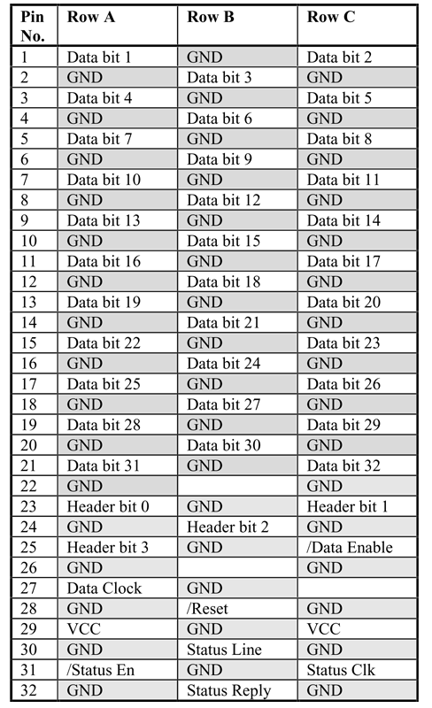
Providing 32 bis data busThe interface caled giga bus, which is the interface between AQ boards and GIGA, but also TIF and GIGA board.
The "SysClk" is 20 MHz. That means a data rate of 80 MB/s can be reached. Pins B30, A31, B32, C31 are for the additional control bus (Status bus), which can be used to setup the not cpu- powered modules like AQ boards. |
 |
|
|
|
||
 |
|
|
SIEMENS V23806, integrated serial/parallel encoder and decoderCompact integrated transceiver unit with: |
||
|
|
||
|
|
|
|
Video input interfaceSixteen differential viedeo input interface. +/- "Ux" are the power supply for the detector board. +5V was an option for the digital power supply, which is never used. CtrlSignal is an option for the identification of detector board, but it does not used.
|
 |
|
|
|
||
Monitoring of input signals:Signal plus +. Signal minus - Differential signal of both signal plus and minus. Push button to change to the next channel. Convert signal |
 |
|
|
|
||
 |
|
|
The chopper control input of sequencer:The chopper control inputs are on the sequencer front panel auxiliary connector. Two inputs are provided, one for the positive chopper phase and the other for the negative. The lines are named Trigger 1 Kathode and Trigger 1 Anode and Trigger 2 Kathode and Trigger 2 Anode four opto de-coupled lines for TTL level drive signals with minimum pulse width of 2 us (The inputs are at the diodes of an optocoupler with a 1K resistor in series). |
 |
|
|
|
||
The interface between sequencer and Cldc board. 16 digital signals are connected over the backplane to each Cldc board.1- Pins A2 to A9 and C2 to C2 are the input interface for Cldc number one. 2- Pins A10 to A17 and C10 to C17 are the input interface for Cldc number two. 3- Two convert pulses (A18, C18) go to tow AQ modules group. 4- Two optinal signals (A20, C20) are only for the future implementation connected to AQ modules, which are currently not used. |
 |
|
Sequencer convert pulse:The convert pulse comes from Sequencer, which starts the data convertion by each ADC. |


Video input interfaceFour differential viedeo input interface. +/- "Ux" are the power supply for the detector board. +5V was an option for the digital power supply, which is never used. CtrlSignal is an option for the identification of detector board, but it does not used.
|
 |
|
|
|
||
Monitoring of video input signals:Signal plus +. Signal minus - Differential signal of both signal plus and minus. Push button to change to the next channel. Convert signal |
||
|
||
|
|
||
 |
|
|