Preliminary CCD tests
CCD Test report
EEV 44-82
CCD name : Bruce
Serial number : 7173-3-1
Type : Backside, Single layer AR Pixel size 15x15 µm
Number of photosensitive pixels 2048 x 4102 [HxV]
Number of outputs : 2
Overall rating : Science
Tested on March 2000
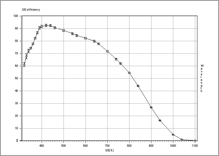
Quantum Efficiency, PRNU
Clock mode: read 350kps LR stripe512

Conversion Factor=   1.8586e-/ADU  ±0.006116     for 23011.2ADU

RMS noise        =   4.0441e-      ±0.3508


CCD temperature : -140Cº


Window area is : X1= 59 X2= 1066 Y1= 9 Y2= 510

Bandwidth 5nm


Wav.       PRNU rms%       QE%

320        1.7             60.8     ±1.7

330        1.5             67.5     ±1.9

340        1.4             71.9     ±1.4

350        1.4             74.0     ±0.7

360        1.4             77.6     ±0.7

370        1.3             82.0     ±0.8

380        1.1             86.3     ±0.8

390        1.0             90.3     ±0.9

400        0.9             91.5     ±0.9

420        0.8             92.2     ±0.9

440        0.8             92.1     ±0.9

460        0.7             90.4     ±0.9

500        0.7             88.2     ±0.8

540        0.7             85.7     ±0.8

560        0.7             84.1     ±0.8

600        0.7             81.9     ±0.8

640        0.7             79.6     ±0.7

660        0.7             77.5     ±0.7

700        0.9             71.5     ±0.6

740        1.0             65.2     ±0.5

760        1.2             61.7     ±0.5

800        1.6             54.3     ±0.4

840        2.1             43.9     ±0.3

900        2.5             26.6     ±0.2

940        3.9             16.1     ±0.12

1000       7.5             4.65     ±0.03

1040       8.1             0.8      ±0.005

1100       11.7            0.09     ±0.0006
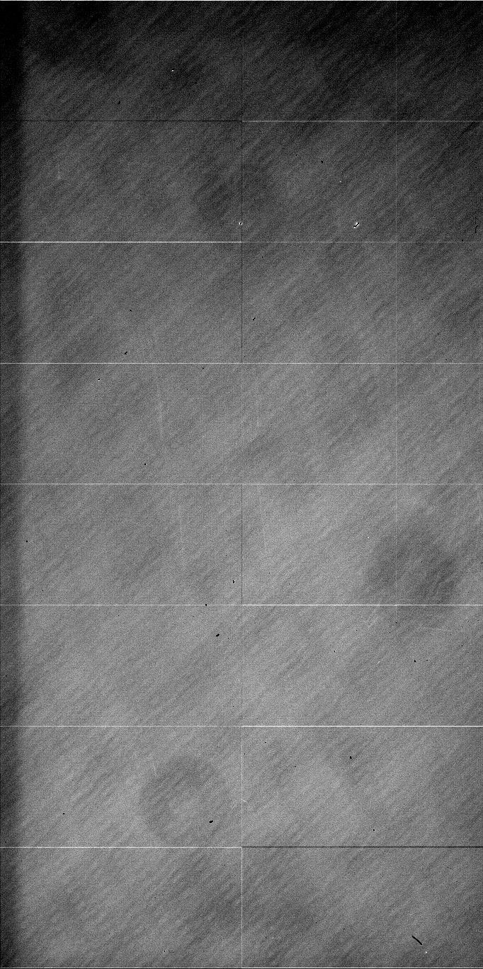
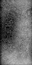
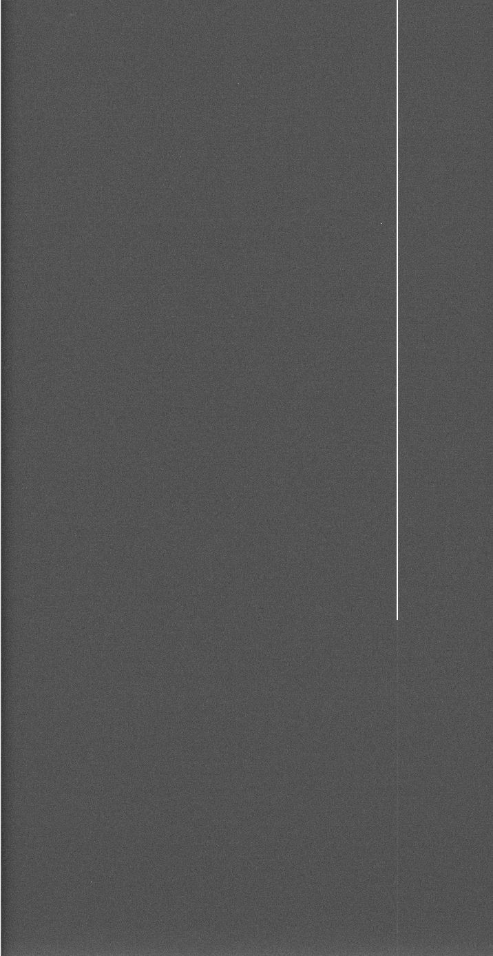
Cosmetic defects
flat field
350nm (UV), bandwidth 5nm
High level
Low level
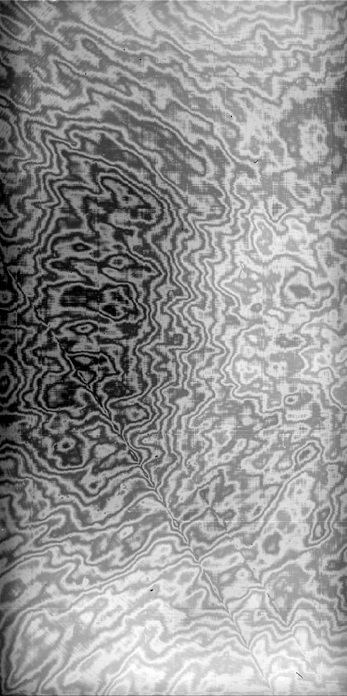
600 nm, bandwidth 5nm
High level
Low level
900 nm, bandwidth 5nm
High level
Low level
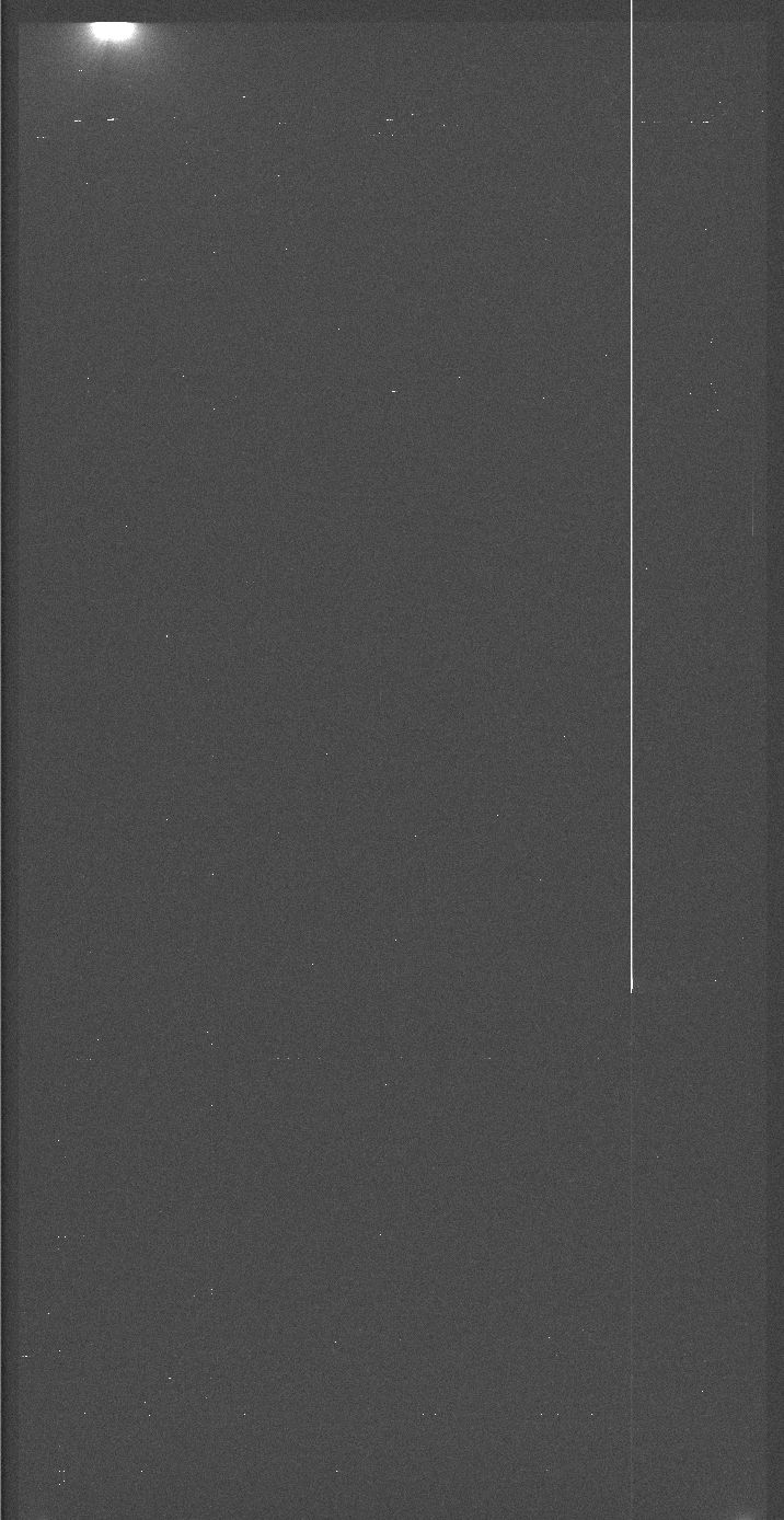
Type of defect Location (x,y) Number of pixels affected Hot pixel x=1680, y=1466 2500*3 Bias
Type of defect Location Number of pixels affected Hot pixel x=1680, y=1466 2500*3
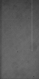
Long exposure dark image
A glowing in the top is visible, nothing related with amplifier glowing. It looks like charge injection on the top of the device


Cross section of this effect (ADUs):
Type of defect Location Number of pixels affected Hot pixel x=1680, y=1466 2500*3 Glowing Upper left ---- Readout noise/Conversion factor
Read out speed: 166kps

Left readout port

Conversion Factor=   1.722e-/ADU  ±0.006     for 27149.6ADU

RMS noise        =   3.84e-       ±0.28


Readout speed: 166kps

Right readout port

Conversion Factor=   1.721e-/ADU  ±0.006     for 27065.1ADU

RMS noise        =   4.19e-       ±0.30


Read out speed: 350kps

Left readout port

Conversion Factor=   1.867e-/ADU  ±0.006     for 26889.9ADU

RMS noise        =   4.08e-       ±0.35


Read out speed: 350kps

Right readout port

Conversion Factor=   1.864e-/ADU  ±0.006     for 26832.2ADU

RMS noise        =   4.58e-       ±0.39
Linearity (TDI method)
not done
Dark current
not done
Charge Transfer Efficiency (CTE)
Horizontal CTE = 0.9999988

Vertical CTE   = 0.9999997