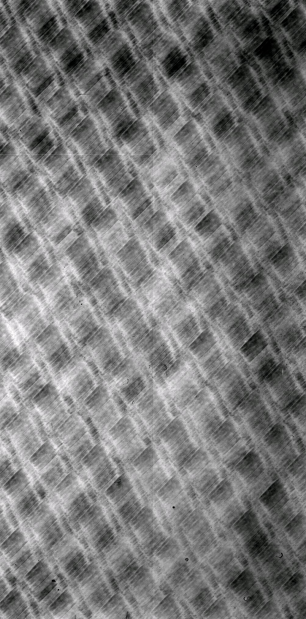
Low Level Flat Field
Mean number of electrons per pixel » 4.000 |
| Type of Defect : |
Location (x,y) : |
Number of pixels affected : |
| Hot column |
63,2831 |
Up to the top |
| Trap |
82,3227 |
10 pixels wide, to the top |
| Trap |
937,2938 |
Up to the top |
| Trap |
1605,827 |
Up to the top |
|
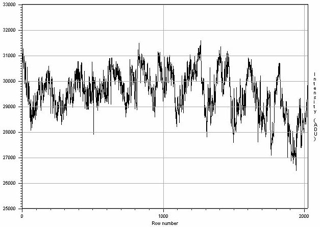
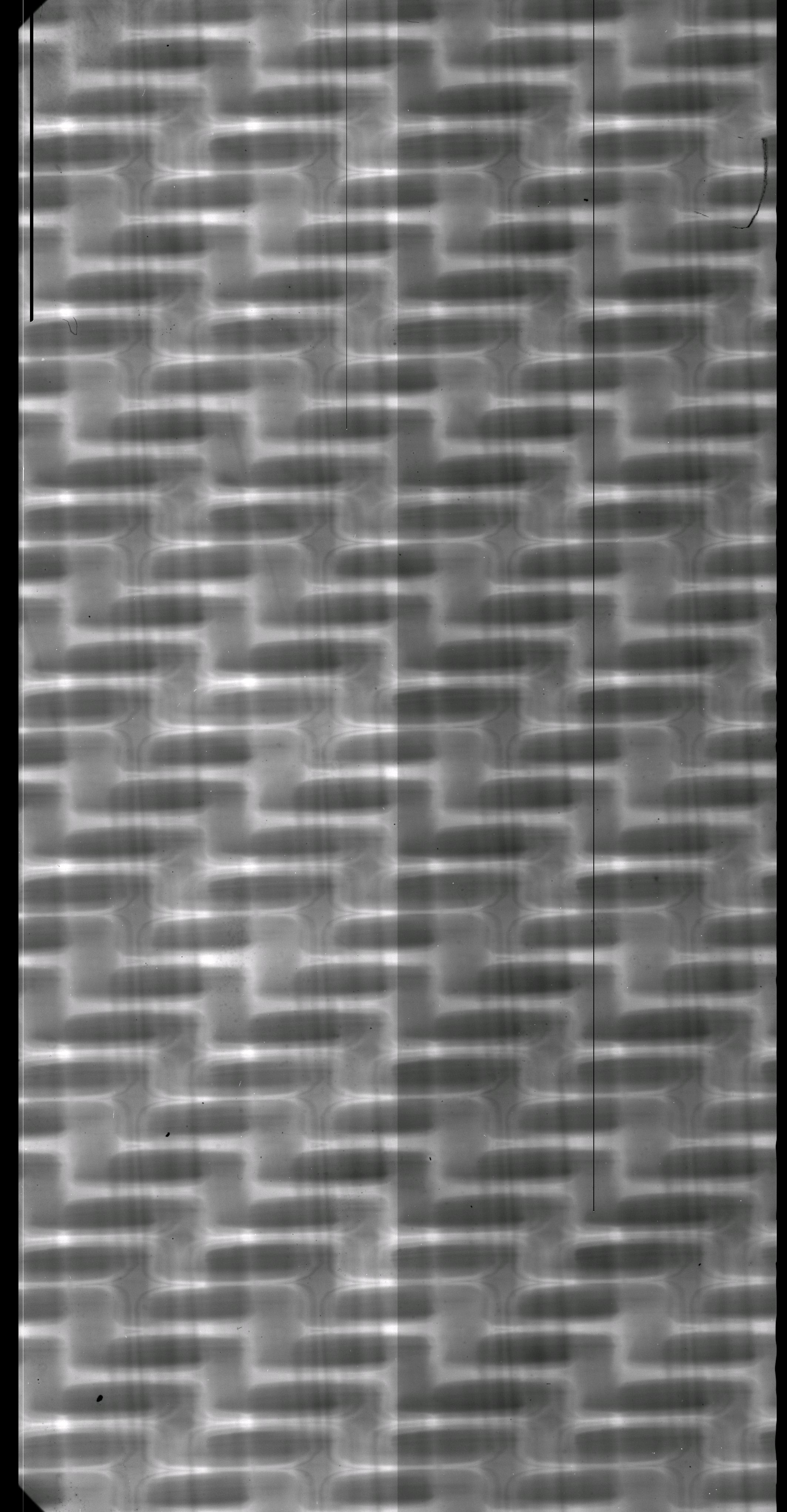
Long Exposure Dark Images
5 exposures of 3.600 sec. each, 2.432 pixels above 5 s
|
| Type of Defect : |
Location (x,y) : |
Number of pixels affected : |
| Defect column |
6,1 |
Whole column |
| Very hot pixels + trail |
8,2692 |
» 200 |
| Trap, 1 pixel wide, to the top |
79,1223 |
y = 1223 to the top |
| Trap, 1 pixel wide, to the top |
1548,803 |
y = 803 to the top |
| Trap, 1 pixel wide, to the top |
881,2914 |
y = 2914 to the top |
| Trap, 10 pixels wide, to the top |
31,3207 |
y = 3207 to the top |
|