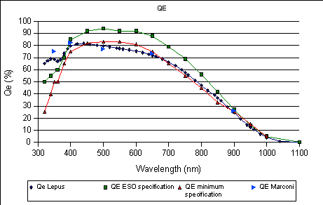
Figure 1: Comparison between the QE measured by ESO, the QE measured by Marconi, ESO specification and minimum specification.
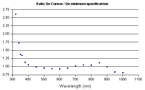
Figure 2: Ratio between the ESO measurements and the ESO minimum specification.
Measurement made by Fabrice Christen
the: 10/05/2002
Data reduced by
Fabrice Christen the: 06/06/2002
Clock mode: 225kpx/rr/HG/512
Conversion Factor=   1.16e-/ADU  ±0.001     for 23643.3ADU
RMS noise        =   6.1e-      ±0.1

CCD temperature : -120.2Cº


Bandwidth 5nm
|
Wav. |
Qe Lepus |
Error |
PRNU (Rms%) |
|
320 |
65.2 |
0.1 |
3.74 |
|
330 |
67.3 |
0.1 |
3.6 |
|
340 |
68.9 |
0.1 |
3.53 |
|
350 |
68.5 |
0.1 |
3.56 |
|
360 |
67.1 |
0.1 |
3.55 |
|
370 |
68.4 |
0.1 |
3.19 |
|
380 |
73.5 |
0.1 |
2.48 |
|
390 |
77.2 |
0.1 |
2 |
|
400 |
79.6 |
0.1 |
1.75 |
|
420 |
81.4 |
0.1 |
1.51 |
|
440 |
81.5 |
0.1 |
1.42 |
|
450 |
81.4 |
0.1 |
1.4 |
|
460 |
81.2 |
0.1 |
1.38 |
|
480 |
80.3 |
0.1 |
1.36 |
|
500 |
79.6 |
0.1 |
1.34 |
|
520 |
78.8 |
0.1 |
1.34 |
|
540 |
78.0 |
0.1 |
1.34 |
|
550 |
77.5 |
0.1 |
1.34 |
|
560 |
77.0 |
0.1 |
1.34 |
|
580 |
76.3 |
0.1 |
1.35 |
|
600 |
75.4 |
0.1 |
1.37 |
|
620 |
74.1 |
0.1 |
1.4 |
|
640 |
72.7 |
0.1 |
1.43 |
|
650 |
71.9 |
0.1 |
1.45 |
|
660 |
71.0 |
0.1 |
1.46 |
|
680 |
68.9 |
0.1 |
1.5 |
|
700 |
66.4 |
0.2 |
1.54 |
|
720 |
63.3 |
0.1 |
1.61 |
|
740 |
59.8 |
0.1 |
1.64 |
|
750 |
57.7 |
0.1 |
1.68 |
|
760 |
55.6 |
0.1 |
1.72 |
|
780 |
51.2 |
0.1 |
1.73 |
|
800 |
47.0 |
0.1 |
1.77 |
|
820 |
42.7 |
0.1 |
1.77 |
|
840 |
39.1 |
0.1 |
1.74 |
|
850 |
36.8 |
0.04 |
1.82 |
|
860 |
34.5 |
0.02 |
1.9 |
|
880 |
29.3 |
0.03 |
1.78 |
|
900 |
24.8 |
0.02 |
2.23 |
|
920 |
19.3 |
0.02 |
2.1 |
|
940 |
14.5 |
0.01 |
2.03 |
|
950 |
12.6 |
0.01 |
2.29 |
|
960 |
10.6 |
0.01 |
2.55 |
|
980 |
6.9 |
0.003 |
2.03 |
|
1000 |
4.07 |
0.01 |
1.97 |
|
1040 |
0.692 |
0.001 |
2.64 |
|
1100 |
0.0687 |
0.0003 |
5.46 |
Table 1: Measurement of the Quantum Efficiency.
In this section you can compare the QE we measured with the testbench and:
QE Minimum specification
Typical QE
QE from Marconi
|
|
|
|---|---|
Figure 1: Comparison between the QE measured by ESO, the QE measured by Marconi, ESO specification and minimum specification. |
Figure 2: Ratio between the ESO measurements and the ESO minimum specification. |
|
Special specification |
|||
|
Wavelength(nm) |
Minimum spec. (%) |
ESO measurements (%) |
Result |
|
350 |
50 |
68.5 |
OK |
|
400 |
80 |
79.6 |
Under the minimum spec. |
|
650 |
80 |
71.9 |
Under the minimum spec. |
|
900 |
25 |
24.8 |
Under the minimum spec. |
|
Conclusion: |
No this ccd is not in the 25% |
||
Table 2: Minimum specification for 25% of the ccds.
|
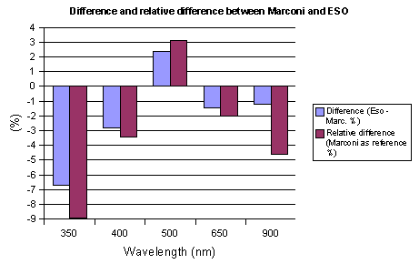
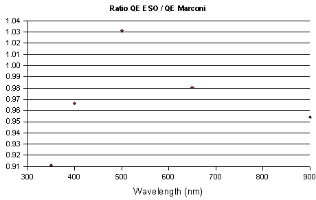
Comparison QE ESO and QE Marconi |
|||||
|
Wavelength (nm) |
QE ESO (%) |
Qe Marconi (%) |
Difference (Eso - Marc. %) |
Relative difference (Marconi as reference %) |
Ratio QE ESO / QE Marconi |
|
350 |
68.5 |
75.2 |
-6.7 |
-8.9 |
0.91 |
|
400 |
79.6 |
82.4 |
-2.8 |
-3.4 |
0.97 |
|
500 |
79.6 |
77.2 |
2.4 |
3.1 |
1.03 |
|
650 |
71.9 |
73.3 |
-1.5 |
-2.0 |
0.98 |
|
900 |
24.8 |
26 |
-1.2 |
-4.6 |
0.95 |
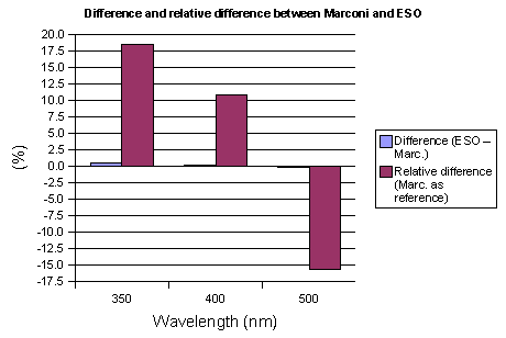
Table 3: Difference and relative difference between ESO measurements and Marconi.
|
|
|
|---|---|
Figure 3: Graphic representation of the difference and the relative difference. |
Figure 4: Ratio between the ESO measurements and the Marconi measurements |
In this section you can compare the PRNU we measured at ESO and:
PRNU Minimum specification
PRNU from Marconi
|
|
|
|---|---|
|
Figure 5: Comparison between the PRNU measured by ESO, the PRNU measured by Marconi, and the maximum specification. |
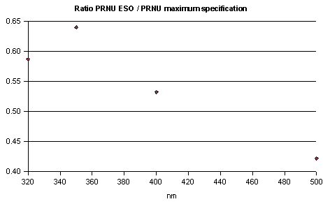
Figure 6: Ratio between the ESO measurements and the Maximum specification. |
|
|
|
|
Figure 7: Graphic representation of the difference and the relative difference. |
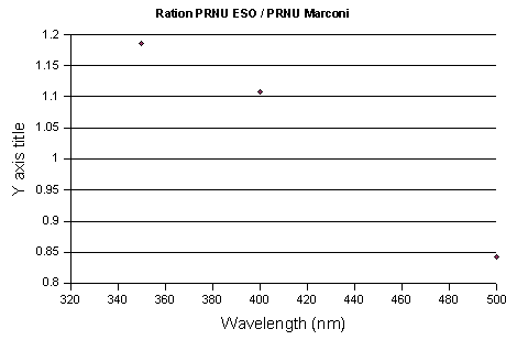
Figure 8: Ratio between the ESO measurements and the Marconi measurements. |
|
Comparison PRNU ESO and PRNU Marconi |
||||||
|
Wavelength (nm) |
PRNU ESO (rms %) |
Maximum spec. |
PRNU Marconi |
Difference (ESO – Marc.) |
Relative difference (Marc. as reference) |
Ratio PRNU ESO / PRNU Marconi |
|
320 |
3.52 |
6 |
/ |
/ |
/ |
/ |
|
350 |
3.2 |
5 |
2.7 |
0.5 |
18.52 |
1.19 |
|
400 |
1.33 |
2.5 |
1.2 |
0.13 |
10.83 |
1.11 |
|
500 |
0.84 |
2 |
1 |
-0.16 |
-15.7 |
0.84 |
Table 4 : Difference and relative difference between ESO measurements and Marconi.
In this section you will see the if the values we have measured for the QE and the PRNU are in accordance with the contract.
|
Wavelength (nm) |
Qe |
PRNU |
|
320 |
OK |
OK |
|
340 |
OK |
|
|
350 |
OK |
OK |
|
360 |
OK |
|
|
380 |
OK |
|
|
400 |
OK |
OK |
|
450 |
Below the specification |
OK |
|
500 |
Below the specification |
OK |
|
550 |
Below the specification |
|
|
600 |
Below the specification |
|
|
650 |
Below the specification |
|
|
700 |
OK |
|
|
750 |
OK |
|
|
800 |
OK |
|
|
850 |
OK |
|
|
900 |
OK |
|
|
950 |
Below the specification |
|
|
1000 |
Below the specification |
|
Table 5: Comparison between the values we have measured and the specifications in the contract.
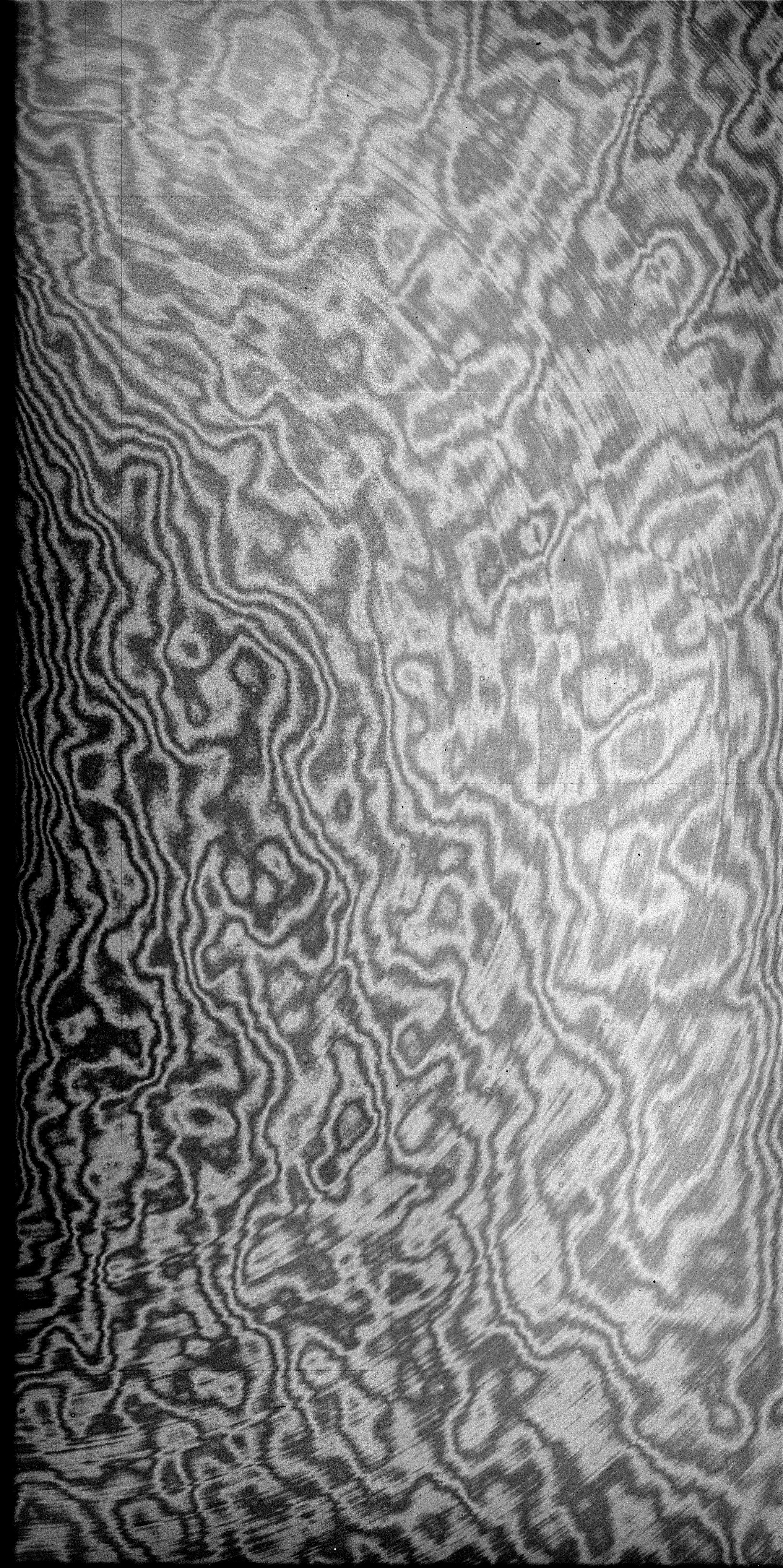
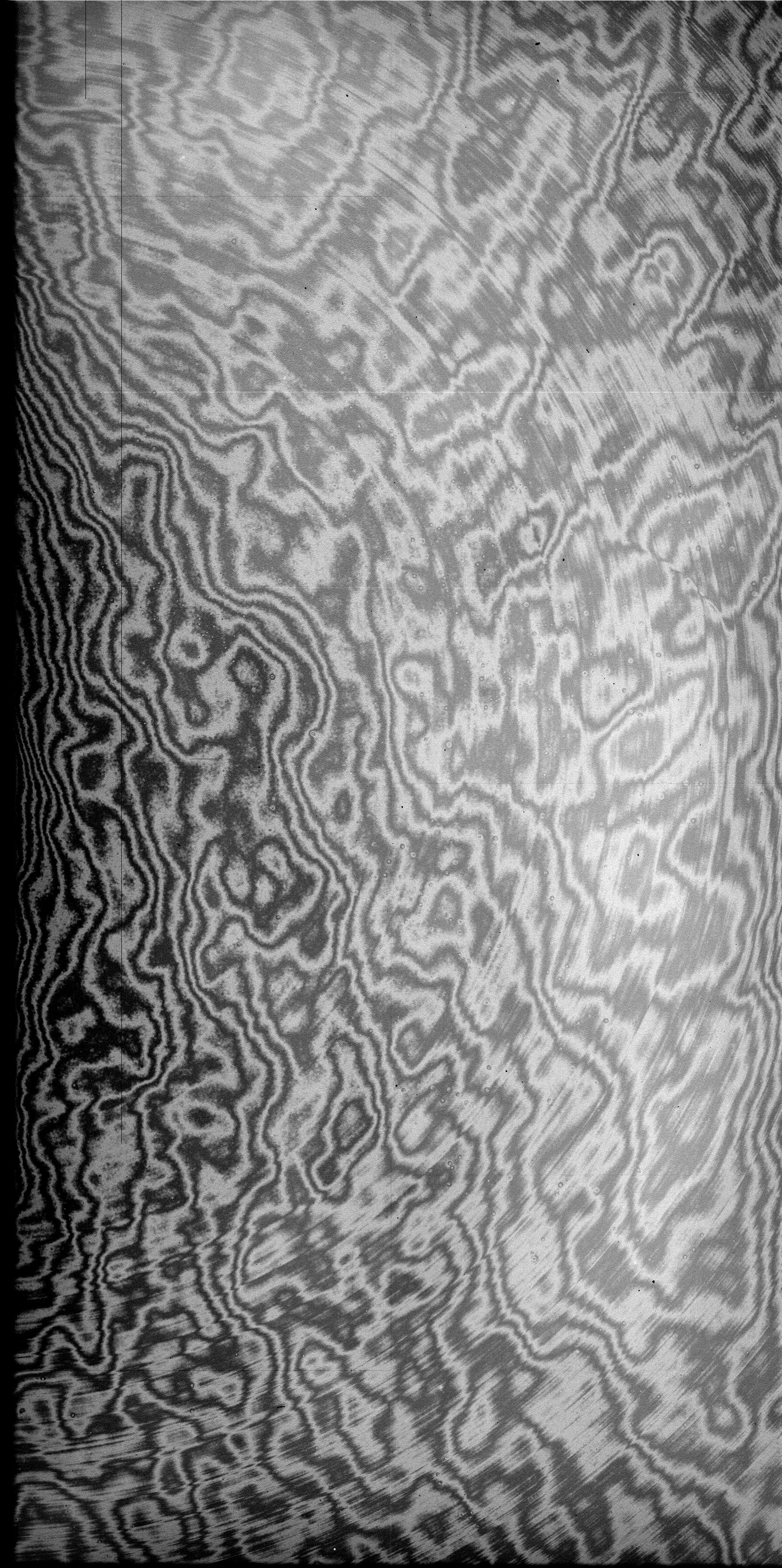
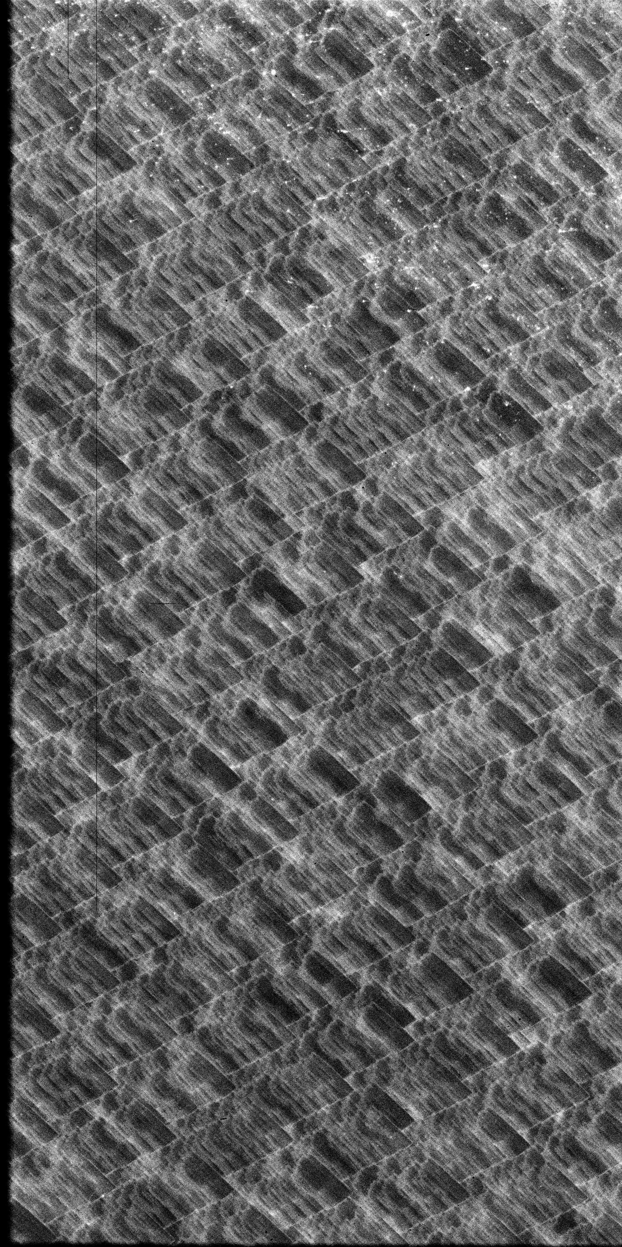
For the flat field we use three wavelengths, 350nm, 600nm and 900nm. For each wavelength we make two images, high level (45000 ADU) and low level (1000 ADU).
350nm (UV), Bandwidth 5nm, High gain mode, High level |
475nm, Bandwidth 5nm, High gain mode, High level |
600nm, Bandwidth 5nm, High gain mode, High level |
750nm, Bandwidth 5nm, High gain mode, High level |
900nm, Bandwidth 5nm, High gain mode, High level |
|||||
|
|
|
|
|
|
|
|
|
|
|
350nm (UV), bandwidth 5nm, High gain mode, Low level |
475nm, bandwidth 5nm, High gain mode, Low level |
600nm, bandwidth 5nm, High gain mode, Low level |
750nm, bandwidth 5nm, High gain mode, Low level |
900nm, bandwidth 5nm, High gain mode, Low level |
|||||
|
|
|
|
|
|
|
|
|
|
|
350nm (UV), bandwidth 5nm, Low gain mode, High level |
475nm (UV), bandwidth 5nm, Low gain mode, High level |
600nm (UV), bandwidth 5nm, Low gain mode, High level |
750nm (UV), bandwidth 5nm, Low gain mode, High level |
900nm (UV), bandwidth 5nm, Low gain mode, High level |
|||||
|
Not available |
Not available |
Not available |
Not available |
Not available |
Not available |
Not available |
Not available |
Not available |
Not available |
350nm (UV), bandwidth 5nm, Low gain mode, Low level |
475nm (UV), bandwidth 5nm, Low gain mode, Low level |
600nm (UV), bandwidth 5nm, Low gain mode, Low level |
750nm (UV), bandwidth 5nm, Low gain mode, Low level |
900nm (UV), bandwidth 5nm, Low gain mode, Low level |
|||||
|
Not available |
Not available |
Not available |
Not available |
Not available |
Not available |
Not available |
Not available |
Not available |
Not available |
Table 6: Flat field for three wavelengths.
The time exposure, for the long dark exposure, is 3600 seconds.
|
Bias 50 kpix/s High Gain |
Bias 225 kpix/s High Gain |
Bias 625 kpix/s High Gain |
Bias 225 kpix/s Low Gain |
|---|---|---|---|
|
|
|
|
|
|
Dark 15min 50 kpix/s High Gain |
Dark 15min 225 kpix/s High Gain |
Dark 15min 625 kpix/s High Gain |
Dark 15min 225 kpix/s Low Gain |
|---|---|---|---|
|
|
|
|
|
|
Dark 1 hour 50 kpix/s High Gain |
Dark 1 hour 225 kpix/s High Gain |
Dark 1 hour 625 kpix/s High Gain |
Dark 1 hour 225 kpix/s Low Gain |
|---|---|---|---|
|
|
|
|
|
Table 7: Bias and dark.
Clock mode: 50kpx/rlrl/HG/512
Left readout port
Conversion Factor=   0.48 e-/ADU ± 0.01     for 20167.2 ADU
RMS noise        =   3.2 e-      ± 0.2
Right readout port
Conversion Factor=   0.49 e-/ADU  ± 0.01     for 20060.7 ADU
RMS noise        =   3.4 e-      ± 0.2

Clock mode: 225kpx/rlrl/HG/512
CCD 1
Left readout port
Conversion Factor=   0.49 e-/ADU ± 0.01     for 20365 ADU
RMS noise        =   4.2 e-      ± 0.2
Right readout port
Conversion Factor=   0.50 e-/ADU  ± 0.01     for 20164.1 ADU
RMS noise        =   5.1 e-       ± 0.3
RMS non linearity (%)         =  0.11
Peak to peak non linearity (%)=  0.35
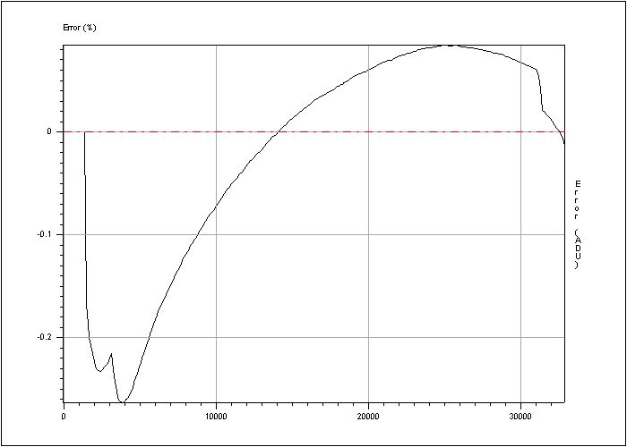
Figure 9: Error of linearity
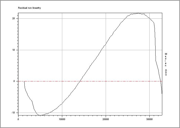
Figure 10: Residual non linearity.
Exposure time (s) = 3600
Dark current : 1.32 ± 0.03 e-/hour/pixel
|
|
CTE (ESO) |
CTE (Marconi) |
|---|---|---|
|
CTE Serial (Horizontal) Left |
/ |
0.999996 |
|
CTE Serial (Horizontal) Right |
0.999993 |
0.999996 |
|
CTE Parallel (Vertical) |
0.9999992 |
0.999998 |
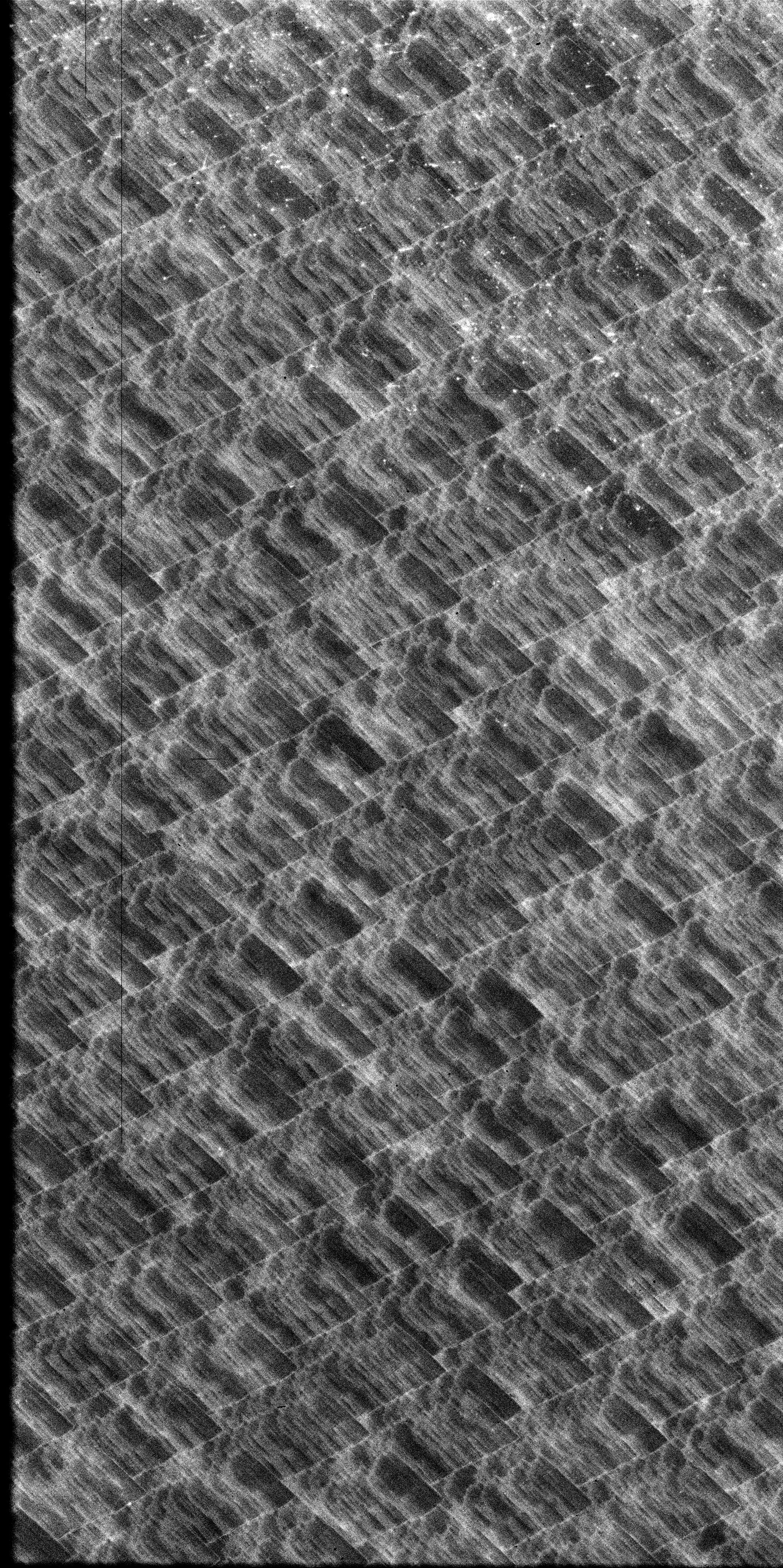
In this section we expose the hot pixel, the dark pixel, the trap and the very large trap we found.
A hot pixel provides a signal of > 60 e- / pixel / hour.
Result: 48 hot points.
a very bright pixel provides a signal of > 200000 e-/pixel/hour
Result: 0 very bright pixel.
A dark pixel is one with 50% or less than the average output for uniform intensity light level, measured with a flat field level around 500 photo-electrons.
Result: 6 dark pixels detected.
A trap is defined as a pixel that captures more than 10 electrons, measured with a flat field level around 500 photo-electrons.
Result: 0 trap
A very large trap is defined as a pixel that captures more than 10 000 electrons, measured with a flat field level around 90% of full well capability.
Result: / very large trap.
A bad column is 10 or more contiguous hot or dark pixels in a single column or a very bright pixel or a very large trap.
Result: 2 bad columns.
Here is a summary of cosmetic defects:
|
|
Hot pixel |
Dark pixel |
A very bright pixel (a) |
Trap |
Very large trap (b) |
Sup. 10 contiguous pixels (c) |
Total bad column (a+b+c) |
|---|---|---|---|---|---|---|---|
|
ESO |
48 |
6 |
0 |
5 |
/ |
2 |
2 |
|
Marconi |
35 |
6 |
3 |
5 |
1 |
12 |
|
Table 8: Summary of cosmetic defects.
###############################################################################
#Author:        Cyril CAVADORE
#CAMERA:        Double Marconi   ( Mosaic 2 Marconi/EEV )
#Purpose:       This is the global voltage definition table micro sequences
#               European Southern Observatory (ESO)
#Date:          20.11.00
###############################################################################
#  GOBAL VOLTAGE DEFINITION TABLE
#
# This table defines the voltages which will be applied to peripherals
# at initialisation time. It also defines the high and low limits which may
# be set for these voltages
###############################################################################
# BRD_ID  PERIPH_ID                LOW    HIGH   TOLERANCE   INIT_VAL
#
# Anabias voltages are in 0.001 volts
#
###############################################################################
#  BIASBRD 0 is for the EEV CCD-44 in the mosaic
###############################################################################
# BRD_ID  PERIPH_ID                LOW    HIGH   TOLERANCE   INIT_VAL

# CONNECTOR P0 - A

BRD_ANABIAS0 ANB_PRESET_VOLT_A   -3500   -1000       10000      -3000   #OG1R  VOG1
BRD_ANABIAS0 ANB_PRESET_VOLT_B   -2500   -1000       10000      -2000   #OG2R  VOG2
BRD_ANABIAS0 ANB_PRESET_VOLT_C    2000   25000       10000      22000   #ODR   VOD
BRD_ANABIAS0 ANB_PRESET_VOLT_D    2000   15000       10000      11000   #RDR   VRD
BRD_ANABIAS0 ANB_PRESET_VOLT_E    2000   25000       10000      24000   #JDR   JFETVoltage
BRD_ANABIAS0 ANB_PRESET_VOLT_F       0       0           0          0   #not used
BRD_ANABIAS0 ANB_PRESET_VOLT_G       0       0           0          0   #not used
BRD_ANABIAS0 ANB_PRESET_VOLT_H       0       0           0          0   #not used

# CONNECTOR PO - B

BRD_ANABIAS0 ANB_PRESET_VOLT_I   -3500   -1000       10000      -3000   #OG1L  VOG1
BRD_ANABIAS0 ANB_PRESET_VOLT_J   -2500   -1000       10000      -2000   #OG2L  VOG2
BRD_ANABIAS0 ANB_PRESET_VOLT_K    2000   25000       10000      22000   #ODL   VOD
BRD_ANABIAS0 ANB_PRESET_VOLT_L    2000   15000       10000      11000   #RDL   VRD
BRD_ANABIAS0 ANB_PRESET_VOLT_M    2000   25000       10000      24000   #JDL   JFETVoltage
BRD_ANABIAS0 ANB_PRESET_VOLT_N       0       0           0          0   #not used
BRD_ANABIAS0 ANB_PRESET_VOLT_O    2000   19000       10000      18000   #DDLR  VDD
BRD_ANABIAS0 ANB_PRESET_VOLT_P       0       0           0          0   #not used


#The anabias board also has an opto isolated peripheral

BRD_ANABIAS0 ANB_OPTOOUT             0   32767           4       255


#
################################################################################
# Clock driver rail voltages are in 0.001 volts
#
################################################################################
#CLOCKDRIVER BOARD 0 is for the EEV CCD44 in the mosaic
################################################################################
#
#
# BRD_ID       PERIPH_ID        LOW        HIGH     TOLERANCE   INIT_VAL
#
#   CONNECTOR PO-A
#
BRD_CLKDRV0 CLKDRV_DAC0_LO     -5000      -5000     1000       -5000 #SWL  VRPhi
BRD_CLKDRV0 CLKDRV_DAC0_HI      5000       5000     1000        5000
BRD_CLKDRV0 CLKDRV_DAC1_LO     -5000      -5000     1000       -5000 #SWR  VRPhi
BRD_CLKDRV0 CLKDRV_DAC1_HI      5000       5000     1000        5000
BRD_CLKDRV0 CLKDRV_DAC2_LO     -5000      -5000     1000       -5000 #RF3  VRPhi
BRD_CLKDRV0 CLKDRV_DAC2_HI      5000       5000     1000        5000
BRD_CLKDRV0 CLKDRV_DAC3_LO     -5000      -5000     1000       -5000 #RF2L VRPhi
BRD_CLKDRV0 CLKDRV_DAC3_HI      5000       5000     1000        5000
BRD_CLKDRV0 CLKDRV_DAC4_LO     -5000      -5000     1000       -5000 #RF1L VRPhi
BRD_CLKDRV0 CLKDRV_DAC4_HI      5000       5000     1000        5000
BRD_CLKDRV0 CLKDRV_DAC5_LO     -5000      -5000     1000       -5000 #RF2R VRPhi
BRD_CLKDRV0 CLKDRV_DAC5_HI      5000       5000     1000        5000
BRD_CLKDRV0 CLKDRV_DAC6_LO     -5000      -5000     1000       -5000 #RF1R VRPhi
BRD_CLKDRV0 CLKDRV_DAC6_HI      5000       5000     1000        5000
BRD_CLKDRV0 CLKDRV_DAC7_LO     -6000      -6000     1000       -6000 #DG   VDG
BRD_CLKDRV0 CLKDRV_DAC7_HI      6000       6000     1000        6000
#
#     CONNECTOR PO-B
#
BRD_CLKDRV0 CLKDRV_DAC8_LO    -12000      -4000     1000       -7000 #IF1 VIPhi
BRD_CLKDRV0 CLKDRV_DAC8_HI     -2000       3000     1000        3000
BRD_CLKDRV0 CLKDRV_DAC9_LO    -12000      -4000     1000       -7000 #IF2 VIPhi
BRD_CLKDRV0 CLKDRV_DAC9_HI     -2000       3000     1000        3000
BRD_CLKDRV0 CLKDRV_DAC10_LO   -12000      -4000     1000       -7000 #IF3 VIPhi
BRD_CLKDRV0 CLKDRV_DAC10_HI    -2000       3000     1000        3000
BRD_CLKDRV0 CLKDRV_DAC11_LO    -0000      -0000     1000       -0000 #empty
BRD_CLKDRV0 CLKDRV_DAC11_HI     0000       0000     1000        0000
BRD_CLKDRV0 CLKDRV_DAC12_LO    -6000      -4000     1000       -6000 #FRL
BRD_CLKDRV0 CLKDRV_DAC12_HI     6000       8000     1000        6000
BRD_CLKDRV0 CLKDRV_DAC13_LO    -6000      -4000     1000       -6000 #FRR
BRD_CLKDRV0 CLKDRV_DAC13_HI     6000       8000     1000        6000


#
# Gain should be interpreted as follows
# There are two gains, gain1 is on the preamp, gain2 is on the video board.

# Gain1 =
#     3 == 1.5
#     1 == 2.25
#     0 == 3.0
#
# Gain2 =
#     0 = Minimum (2.5)
#     1 = Maximum (12.5)
#
# BRD_ID  PERIPH_ID             LOW    HIGH   TOLERANCE       INIT_VAL
BRD_VIDBRD0 VID_GAIN1_CHAN0       0       3       0               1
BRD_VIDBRD0 VID_GAIN1_CHAN1       0       3       0               1
BRD_VIDBRD0 VID_GAIN1_CHAN2       0       3       0               1
BRD_VIDBRD0 VID_GAIN1_CHAN3       0       3       0               1

BRD_VIDBRD0 VID_GAIN2_CHAN0       0       1       0               0
BRD_VIDBRD0 VID_GAIN2_CHAN1       0       1       0               0
BRD_VIDBRD0 VID_GAIN2_CHAN2       0       1       0               0
BRD_VIDBRD0 VID_GAIN2_CHAN3       0       1       0               0

BRD_VIDBRD0 VID_FILT_CHAN0        0       3       0               0
BRD_VIDBRD0 VID_FILT_CHAN1        0       3       0               0
BRD_VIDBRD0 VID_FILT_CHAN2        0       3       0               0
BRD_VIDBRD0 VID_FILT_CHAN3        0       3       0               0

BRD_VIDBRD0 VID_TESTVID_CHAN0     0       1       0               0
BRD_VIDBRD0 VID_TESTVID_CHAN1     0       1       0               0
BRD_VIDBRD0 VID_TESTVID_CHAN2     0       1       0               0
BRD_VIDBRD0 VID_TESTVID_CHAN3     0       1       0               0

#
# Video Offsets are in 0.001 volts
#
# BRD_ID  PERIPH_ID           LOW    HIGH   TOLERANCE    INIT_VAL
#


BRD_VIDBRD0 VID_OFFSET_CHAN0    0   65535    6553            0
BRD_VIDBRD0 VID_OFFSET_CHAN1    0   65535    6553            0
BRD_VIDBRD0 VID_OFFSET_CHAN2    0   65535    6553            0
BRD_VIDBRD0 VID_OFFSET_CHAN3    0   65535    6553            0
Back to the overview page ESO Test Reports for the OmegaCAM CCDs